DC-DC的选型及应用
目录
名词解释
| 名词 | 解释 |
|---|---|
| DC-DC | DC-to-DC converter 直流转直流转换器 |
| Buck | 降压型转换器 |
| Boost | 升压型转换器 |
写在前面
本文将通过分析手册、PCB实验,挑选合适的DCDC器件
我们选择了一些市面上常见的升压、降压型DCDC器件来进行测试,如下
降压型
JW5211
| 拓扑结构 | 降压式 Buck |
| 输入电压 | 2.5V~5.5V |
| 输出电压 | |
| 输出电流(最大值) | 1.2A |
| 静态电流 | 40uA~60uA |
| 开关频率 | 1.5MHz |
SY8088AAC
| 拓扑结构 | 降压式 Buck |
| 输入电压 | 2.5V~5.5V |
| 输出电压 | |
| 输出电流(最大值) | 1A |
| 静态电流 | 40uA |
| 开关频率 | 1.5MHz |
RY3408
| 拓扑结构 | 降压式 Buck |
| 输入电压 | 2.5V~5.5V |
| 输出电压 | |
| 输出电流(最大值) | 1A |
| 静态电流 | 40uA |
| 开关频率 | 1.5MHz |
升压型
SGM6603-ADJYN6G/TR
立创商城链接:https://item.szlcsc.com/80831.html
The SGM6603 is a constant frequency, current mode, synchronous, step-up switching regulator. Its output currents can go as high as 75mA while using a single-cell alkaline, and discharge it down to 0.9V. It can also be used for generating 5V at 500mA from a 3.3V rail or a Li-ion battery.
手册中多次提及可用于2.5V~4.2V锂电池升压5V的应用
| 拓扑结构 | 升压式 Boost |
| 输入电压 | 900mV~5.5V |
| 输出电压 | 2.5V~5.5V |
| 输出电流(最大值) | |
| 开关频率 | 1.2MHz |
典型应用
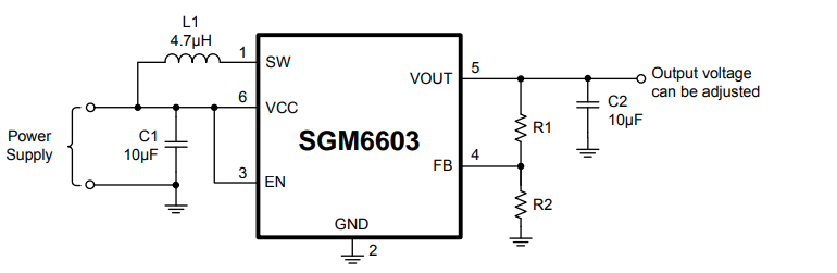
根据手册中的说明,本器件具有防倒灌功能,所以不需要在Vout处加肖特基二极管
输入电压对效率的影响(5V)
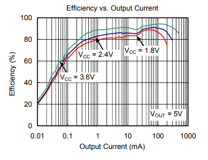
根据图表得知,输入电压大于3.7V时,效率在60%以下,但暂时没有进行验证。
电感的选择
A boost converter normally requires two main passive components for storing energy during the conversion. A boost inductor and a storage capacitor at the output are required. To select the boost inductor, it is recommended to keep the possible peak inductor current below the current limit threshold of the power switch in the chosen configuration. The highest peak current through the inductor and the switch depends on the output load, the input (VCC), and the output voltage (VOUT).
电感与输出电容提供了升压所需的能量,可通过手册中如下公式计算应用电感参数
$I_L = I_O \times \frac{V_{out}}{V_{cc} \ \times \ 0.8} $
本例需要 5.5V 500mA输出,假设输入电压为4V,带入公式计算得,峰值电流为859.3mA,
所需功率电感的峰值电流应为1A。
可选择0805 2.2uH 1A功率电感
https://item.szlcsc.com/356676.html
输入电容的选择
At least a 10µF input capacitor is recommended to improve transient behavior of the regulator and EMI behavior of the total power supply circuit. A ceramic capacitor or a tantalum capacitor with a 100nF ceramic capacitor in parallel, placed close to the IC, is recommended
输出电容的选择
The major parameter necessary to define the output capacitor is the maximum allowed output voltage ripple of the converter. This ripple is determined by two parameters of the capacitor, the capacitance and the ESR. It is possible to calculate the minimum capacitance needed for the defined ripple, supposing that the ESR is zero,
R1/R2电阻的选择
The typical value of the voltage at the FB pin is 500mV. The maximum recommended value for the output voltage is 5.5V.
R1 = R2 * (Vout/500mV - 1)
此例中,需要5.5V输出,经过1n5819ws 0.6V左右压降,得到接近的5V R1 = 10K, R2 = 1K
R2 is recommended to be 100kΩ. For example, if an output voltage of 3.3V is needed, a 560kΩ resistor should be chosen for R1.
根据手册中说明,R2推荐大小100K,那R1就要改为1000K